NOTA RUJUKAN....
How to Understand IC 4017 Pin Outs - Explained in Simple Words
The IC 4017 can be considered as one of the most useful and versatile chip having numerous electronic circuit applications. Technically it is called the Johnsons 10 stage decade counter divider.
So in a way it is counting and also dividing the input clock by 10 and hence the name.
The name suggest two things, it’s something to do with number 10 and counting/dividing.
The number 10 is connected with the number of outputs this IC has, and these outputs become high in sequence in response to every high clock pulse applied at its input clock pin out. It means, all its 10 outputs will go through one cycle of high output sequencing from start to finish in response to 10 clocks received at its input.
So in a way it is counting and also dividing the input clock by 10 and hence the name.

Let’s understand the pin outs of the IC 4017 in details and from a newcomer’s point of view:
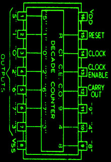
Looking at the figure we see that the device is a 16 pin DIL IC, the pin out numbers are indicated in the diagram with their assignment names.
The pin out which are marked as output are the pins which become logic high one after the other in sequence, meaning the first in the order is 3, so this pin is the one which first becomes high, then it shuts off and simultaneously the next pin #2 becomes, then this pin goes low and simultaneously the preceding pin #4 becomes high and so on until the last pin #11 becomes high and reverts to pin #3 to repeat the cycle.
Please note that the word “high” means a positive voltage that may be equal to the supply voltage of the IC, so when I say the outputs become high in a sequential manner means the outputs produce a positive voltage which shifts in a sequential manner from one output pin to the next, in a “running” DOT manner.
Now the above sequencing or shifting of the output logic from zero to high and back to zero, happens only when a clock signal is applied to the clock input of the IC which is pin #14.
Mind you, if the no clock is applied to this input, it must be assigned either to a positive supply or a negative supply, but should never be kept hanging or unconnected, as per the standard rules for all CMOS inputs.
The clock input pin #14 only responds to positive clocks or a positive signal and with each consequent positive peak signal, the output of the IC shifts or becomes high in sequence, the sequencing of the outputs are in the order of pin outs #3, 2, 4, 7, 10, 1, 5, 6, 9, 11.
Pin #13 may be considered as the opposite of pin #14 and this pin out will respond to negative peak signals, if a clock is applied to this pin, producing the same results with the outputs as discussed above.
However normally this pin out is never used for applying the clock signals, instead pin #14 is taken as the standard clock input.
However, pin #13 needs to be assigned a ground potential, that means, must be connected to the ground for enabling the IC to function. In case pin #13 is connected to positive, the whole IC will stall and the outputs will stop sequencing and stop responding to any clock signal applied at pin #14.
Pin #15 of the IC is the reset pin input. The function of this pin is to revert the sequence back to the initial state in response to a positive potential or supply voltage, meaning the sequencing comes back to pin #3 and begins the cycle afresh, if a momentary positive supply is applied to pin #15.
If the positive supply is held connected to this pin #15, again stalls the output from sequencing and the output clamps to pin #3 making this pin-out high and fixed.
Therefore to make the IC function, pin #15 should always be connected to ground. If this pin out is intended to be used as a reset input, then it may be clamped to ground with a series resistor of 100K or any other high value, so that a positive supply now can be freely introduced to it, whenever the IC is required to be reset.
Pin #8 is the ground pin and must be connected to the negative of the supply, while pin #16 is the positive and should be terminated to the positive of the voltage supply.
Pin #12 is the carry out, and is irrelevant unless many ICs are connected in series, we will discuss it some other day. Pin #12 can be left open.
No comments:
Post a Comment